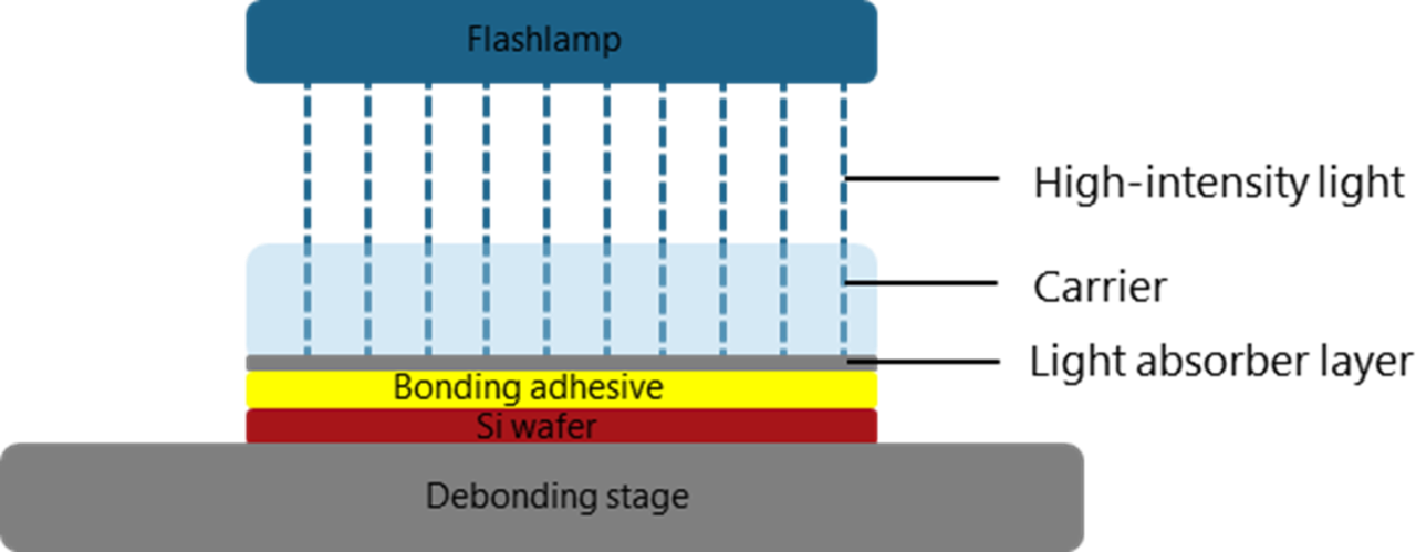
•High-intensity flashlamp source
•Light absorber converts light energy into thermal energy
•Sub-millisecond debond pulse duration
•Debond entire 150 mm wafer with one pulse
•No ash or residue
•High-intensity flashlamps to debond
•Lower processing cost per wafer by at least 30% compared to laser debond
•Cleaner debonding process – no ash or residue
•Significant reduction in cleaning efforts (financial benefit is not reflected in the 30% lower TCO)
•Reusable carriers
•Compatible with warped substrates with significant hardware changes